
Silicon Carbide (SiC) MOSFETs, as representatives of third-generation semiconductor materials, are reshaping the power electronics landscape with their excellent performance. Leakage current, being a critical parameter affecting device reliability, requires particular attention in testing.
SiC MOSFETs are gradually replacing traditional silicon-based devices in fields such as new energy vehicles, photovoltaic inverters, and industrial power supplies due to their high voltage resistance, high-frequency characteristics, and high-temperature operation capability. However, in practical applications, leakage current issues in SiC MOSFETs directly impact the devices' power loss, system reliability, and service life.
Scientifically and accurately testing leakage current is crucial for device selection, circuit design, and application reliability. This article comprehensively introduces the causes, influencing factors, testing methods, and precautions regarding SiC MOSFET leakage current.
1 What is Leakage Current and Why Does It Exist?
Leakage current in SiC MOSFETs primarily refers to the tiny current that still flows from the drain to the source when the device is in the off state. Even when completely turned off under ideal conditions, minute leakage current still exists in practical devices.
1.1 Physical Nature of Leakage Current
In SiC MOSFETs, leakage current mainly consists of the following components:
● pn junction reverse leakage current: Originates from carrier drift and thermal generation effects in the pn junction between drain and source under reverse bias.
● Gate oxide leakage current: Leakage current through the gate oxide layer, closely related to oxide quality and electric field strength.
● Surface leakage current: Current paths along the surface caused by device surface contamination, defects, or imperfections.
1.2 Material Properties and Leakage Current
Although SiC material itself has better performance than silicon, SiC-SiO₂ interface defects are much greater than those in corresponding silicon devices. These interface defects become carrier traps and recombination centers, thereby increasing leakage current.
Neutron radiation experiments show that neutron irradiation with a total fluence of 1.18×10¹¹ cm⁻² does not cause significant degradation of the forward I-V characteristics of SiC SBD, but leads to a significant increase in reverse leakage current.
2 Factors Affecting Leakage Current Magnitude
2.1 Temperature Effects
Leakage current is very sensitive to temperature, increasing exponentially as temperature rises. Studies show that leakage current in SiC MOSFETs at high temperatures may be several orders of magnitude higher than at room temperature.
2.2 Voltage Stress
Leakage current increases with higher drain-source voltage (VDS). Under high voltage stress, avalanche multiplication may occur, further increasing leakage current. The electric field strength in the gate oxide directly affects tunnel current and Fowler-Nordheim tunneling current through the oxide layer.
2.3 Radiation Effects
Radiation introduces defects and traps in SiC materials, leading to increased leakage current. 14 MeV neutron irradiation experiments show that gate current increases significantly in SiC MOSFETs after irradiation (increasing by about
3.3 times at Vgs=15V).
Heavy ion irradiation may cause single event gate rupture (SEGR), a serious leakage current failure mechanism.
2.4 Manufacturing Process and Material Quality
The material's crystallographic quality and defect density directly affect leakage current magnitude. Gate oxide quality is a key factor affecting gate leakage current. Device design and structure (such as cell structure, terminal structure) also affect electric field distribution, thereby influencing leakage current.
3 Leakage Current Testing Methods
3.1 Static Parameter Testing Method
The most direct leakage current testing method is measuring the tiny current between drain and source when the device is off.
Testing requires ensuring:
● The device is completely off (gate-source shorted or off voltage applied)
● Using high-precision source meter unit (SMU) *PLANCK 2300 high voltage SMU can offer minimum measurement resolution up to 1fA/100 uV.
● Controlling stable junction temperature (leakage current is extremely sensitive to temperature)
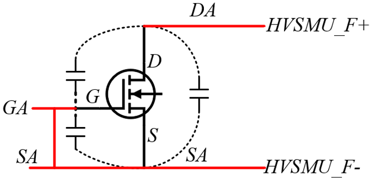
Figure 1 4-Terminal-Kelvin-Force-Sense-Measurement-Setup
3.2 Leakage Current Monitoring in Breakdown Voltage Testing
When testing drain-source breakdown voltage V(BR)DSS, a specific leakage current value (such as 1mA) is usually used as the breakdown criterion.
According to JESD 24:1985 standard, testing should:
● Short the gate to source (Vgs=0V)
● Ensure device case temperature is 25℃
● Gradually increase VDD voltage until reaching stable target current value (such as 1mA)
● Record the VDD value at this point as breakdown voltage
4 Precautions and Common Issues in Leakage Current Testing
4.1 Temperature Control and Measurement
Leakage current is extremely sensitive to temperature, so precise control and measurement of junction temperature is essential during testing. Common issues include:
● Self-heating effects caused by test current
● Environmental temperature fluctuations
● Improper temperature measurement point selection
4.2 Sources of Measurement Error
Test errors are mainly divided into three categories:
● System errors: DC offset, gain error, test hardware design issues
● Quantization errors: Test instrument ADC accuracy limitations
● Random errors: Thermal noise or other noise sources in test hardware
*PLANCK 2300 high voltage SMU can offer minimum measurement resolution up to 1fA/100μV.
*PLANCK 2300 high voltage SMU also offers Guard terminals to eliminate the effects of leakage current that can exist between HI and LO.
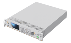
Figure 2 PLANCK 2300 high voltage SMU
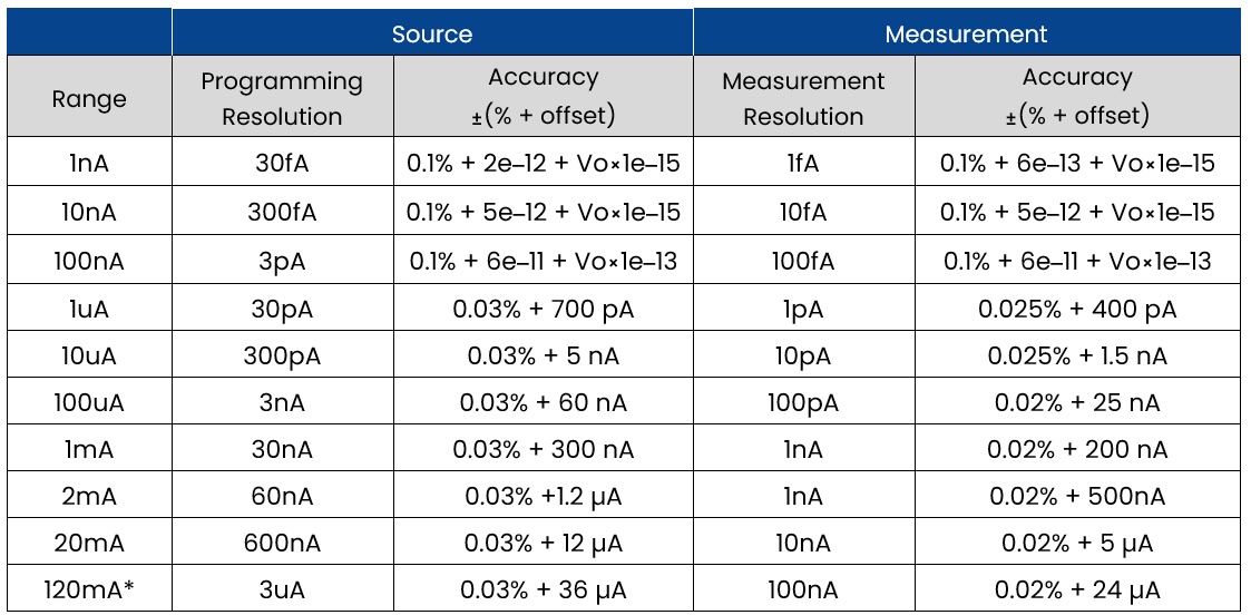
Figure 3 PLANCK 2300 high voltage SMU Specs
4.3 Selection of Test Conditions
Voltage scanning rate needs to be properly controlled, as too fast rates may cause instantaneous overshoot. Test duration needs sufficient consideration, as some leakage mechanisms (such as time-dependent dielectric breakdown of gate oxide) require long testing times.
4.4 Impact of Equipment and Connections
Shielding and grounding are key to microcurrent measurement. Low-noise cables and connectors are required. Electrostatic protection is very important—MOS transistors are easily damaged by static electricity, so anti-static wrist straps must be worn before operation.
5 Summary
SiC MOSFET leakage current testing is a complex process involving multiple factors, requiring comprehensive consideration of device physical characteristics, measurement techniques, temperature effects, and radiation effects.
Choosing the correct testing method, controlling test conditions properly, and understanding the physical principles behind the data are essential for accurately evaluating SiC MOSFET performance.
We hope this article helps you better understand the technical key points of SiC MOSFET leakage current testing and serves as a reference in your power electronic design and testing work.
Thank you for choosing Planck. If you have any business cooperation needs, please feel free to leave a message online. We will properly protect and legally use the information you provide, and arrange for business personnel to contact you as soon as possible!
Thank you for choosing Planck. If you have any business cooperation needs, please feel free to leave a message online. We will properly protect and legally use the information you provide, and arrange for business personnel to contact you as soon as possible!